Multiple Choices Questions (10 pts)
- (2 pts) For the given Verilog testbench snippet, identify X and Y.
module Gate (p, q, r, y);
   input p, q, r;
   output reg y;

   // Module description
endmodule

module Testbench ();
   X
   Y

   Gate Gate_tb (p_tb, q_tb, r_tb, y_tb);
   // Designer-provided input values
   ...
endmodule
- a. X: reg p_tb, q_tb, r_tb; Y: wire y_tb;
- b. X: wire y_tb; Y: reg p_tb, q_tb, r_tb;
- c. X: wire y_tb; Y: always @ (p, q, r);
- d. X: reg p_tb, q_tb, r_tb; Y: always @ (y);
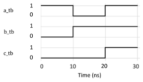
- (2 pts) The given testbench code generates the timing waveform shown in the figure. Identify the correct snippet that must be placed instead of ZZZ to obtain the given waveform.
`timescale 1 ns/ 1 ns
module Lightcontroller (a, b, c);
   input a, b;
   output reg c;

   always @ (a, b) begin
      c = a & b;
   end
endmodule

module Testbench ();
   reg a_tb, b_tb;
   wire c_tb;
   Lightcontroller Lightcontroller_tb (a_tb, b_tb, c_tb);

   Initial begin
         a_tb = 1;
         b_tb = 0;
         ZZZ
         #10 a_tb = 1;
    end

endmodule
- a. #10 a_tb = 0; b_tb = 1;
- b. #20 a_tb = 1; b_tb = 1;
- c. #10 a_tb = 0; #20 a_tb = 1;
- d. #10 a_tb = 0; #10 a_tb = 1;
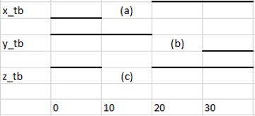
- (2 pts) The given testbench code generates the timing waveform shown in the figure. Identify the values of (a), (b), and (c) in the given waveform.
`timescale 1 ns/ 1 ns
module Motor (x, y, z);
   input x, y;
   output reg z;

   always @ (x, y) begin
          z = x | y;
   end
endmodule

module Testbench ();
   reg x_tb, y_tb;
   wire z_tb;
   Motor Motor_tb (x_tb, y_tb, z_tb);


   Initial begin
         x_tb = 0;
         y_tb = 1;
        #20 x_tb = 1;
         y_tb = 0;
      end


 endmodule
- a. (a) = 0, (b) = 0, and (c) = 1
- b. (a) = 0, (b) = 1, and (c) = 0
- c. (a) = 1, (b) = 0, and (c) = 0
- d. (a) = 1, (b) = 1, and (c) = 1
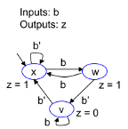
- (2 pts) The given FSM has input b, output z, and starts in state x. What is the FSM’s resulting output if b is 1 on the first rising clock edge, 1 on the second, and 1 on the third?
- a. z = 0
- b. z = 1
- c. z = 01
- d. z = 11
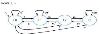
- (2 pts) State F3 transitions to state _____ when enable (e) is 0.
Short-Answer Questions (30 pts)
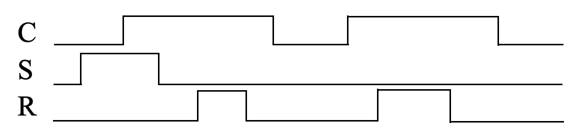
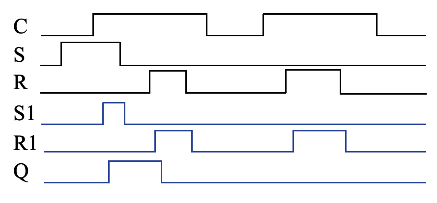
- (5 pts) Trace the behavior of a level-sensitive SR latch for the input pattern in Figure below. Assume S1, R1, and Q are initially 0. Complete the timing diagram, assuming logic gates have a tiny but non-zero delay.
- (5 pts) Using four registers, design a circuit that stores the four values present at an 8-bit input D during the previous four clock cycles. The circuit should have a single 8-bit output that can be configured using two inputs s1 and s0 to output any one of the four registers.
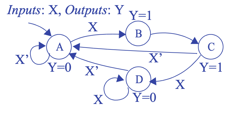
- (5 pts) Draw a state diagram for an FSM that has an input X and an output Y. Whenever X changes from 0 to 1, Y should become 1 for two clock cycles and then return to 0 – even if X is still 1. (Assume for this problem and all other FSM problems that an implicit rising clock is ANDed with every FSM transition condition.)
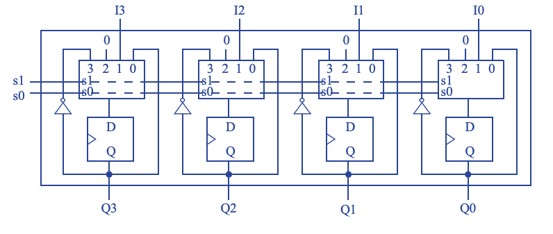
- (5 pts) Design a 4-bit register with 2 control inputs s1 and s0, 4 data inputs I3, I2, I1 and I0, and 4 data outputs Q3, Q2, Q1 and Q0. When s1s0=00, the register maintains its value. When s1s0=01, the register loads I3..I0. When s1s0=10, the register clears itself to 0000. When s1s0=11, the register complements itself, so for example 0000 would become 1111, and 1010 would become 0101.
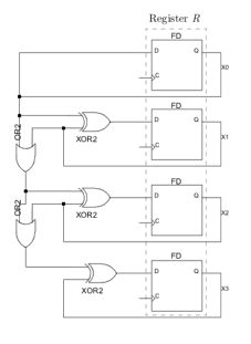
- (5 pts) Let $ \mathbf{X} = \{X3, X2, X1, X0\} $
denote the contents of register R, shown in this circuit, as a two’s complement number. After exactly two clock ticks, what is the contents of R?
$ \mathbf{X} $
- (5 pts) Design a Moore-type state transition diagram for a state machine that has one input (X) and one output (A). The output should go high if the last three instances of X were the same. Otherwise the output should be low. You must use fewer than 9 states.