Midterm 02 (Practice)
Mar 25, 2025
·
3 min read
Multiple Choices Questions (8 pts)
- (2 pts) Which of the following statements is true of testbench?
- a. A testbench consists of one main element named a module.
- b. A testbench provides a sequence of input values to test a module.
- c. A testbench is a module with inputs and outputs.
- d. A testbench creates an instance of a module named with the extension ‘’#tb’’.
- b.
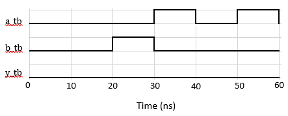
- (2 pts) The testbench for the given Verilog code snippet generates the waveform shown in the figure. Which of the following statements holds true in this case?
- a. y_tb is set to 1 at 30 ns.
- b. y_tb after 30 ns retains a value of 0 until y_tb is assigned a new value.
- c. b_tb is set to 1 at 50 ns.
- d. b_tb after 30 ns retains a value of 0 until b_tb is assigned a new value.
`timescale 1 ns/ 1 ns
module SetTimer (a, b, y);
   input a, b;
   output reg y;


   always @ (a, b) begin
      y = a & b;
   end
endmodule


module Testbench ();
   reg a_tb, b_tb;
   wire y_tb;
   SetTimer SetTimer_tb (a_tb, b_tb, y_tb);

   Initial begin
      a_tb = 0;
      b_tb = 0;
      #20 b_tb = 1;
      #10 a_tb = 1;
      b_tb = 0;
      #10 a_tb = 0;
      #10 a_tb = 1;
    end
endmodule
|
|---|
- d.
- (2 pts) The given FSM has input b, output z, and starts in state m. What is the FSM’s resulting output and state if on the clock’s rising edge b is 0?
- a. z = 0, state = m
- b. z = 1, state = m
- c. z = 0, state = n
- d. z = 1, state = n

|
|---|
- c.
- (2 pts) When implementing the FSM as a controller, how many outputs does the combinational logic block require?
- a. 2
- b. 3
- c. 4
- d. 6

|
|---|
- c.
Short-Answer Questions (40 pts)
- (5 pts) Compare the behavior of D latch and D flip-flop devices by completing the timing diagram in Figure below. Provide a brief explanation of the behavior of each device. Assume each device initially stores a 0.

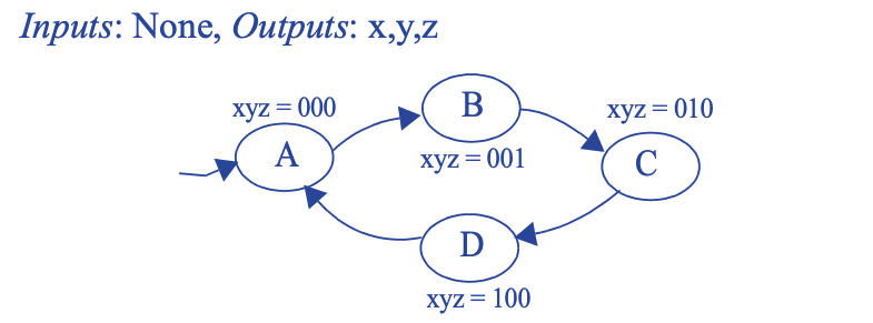
- (5 pts) Draw a state diagram for an FSM with no inputs and three outputs x, y, and z. xyzshould always exhibit the following sequence: 000, 001, 010, 100, repeat. The output should change only on a rising clock edge. Make 000 the initial state.
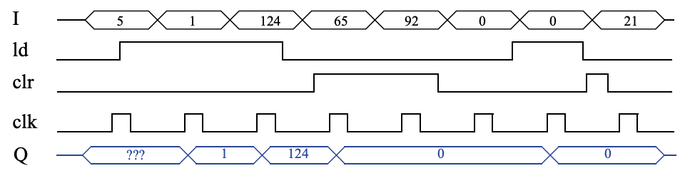
- (5 pts) Trace the behavior of an 8-bit parallel load register with 8-bit input I, 8-bit output Q, load control input ld, and synchronous clear input clr by completing the timing diagram in the figure below.
- (5 pts) Draw the gate level design of a 1-bit full adder. Draw the schematic of a 8-bit carry-ripple adder using eight 1-bit full adders. Assuming AND gates have a delay of 2 ns, OR gates have a delay of 1 ns, and XOR gates have a delay of 3 ns, compute the longest time required to add two numbers using an 8-bit carry-ripple adder.


From the illustration above, we see that both the FA and HA have a maximum gate delay of 3 ns. Therefore, 8 adders * 3 ns/adder = 24 ns is required for an 8-bit carryripple adder to ensure a correct sum is on the adder’s output.
An answer of 23 ns is also acceptable since the carry out of a half-adder will be correct after 2 ns, not 3 ns, and a half-adder may be used for adding the first pair of bits (least significant bits) if the 8-bit adder has no carry-in.
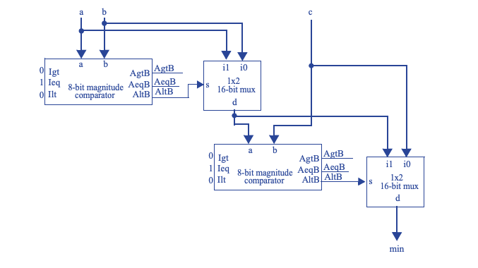
- (5 pts) Use magnitude comparators and logic to design a circuit that computes the minimum of three 8-bit numbers.