This page is subject to change without notice -- please reload it
in your browser if an item that might affect you may have changed.
You will only get credit for this lab if the TA checks you off for the lab 6 assignments listed below no later than Friday, November 14th. The lab 7 assignments are due Wednesday, November 26th.
You must do this lab with your lab group, or individually if you are not part of a lab team. All team members must participate in the design and construction, and all must be present for the evaluation.
The datasheet for almost all the circuits used in this lab are available from Texas Instruments. The only other circuit is the memory. I have selected a non-volatile program RAM, the DS1225AB, which is documented here and a volatile data RAM, the 74F189, which is documented here
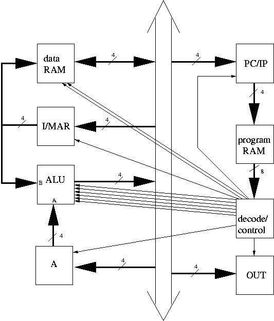
In these two projects, you will build a very simple computer, similar in complexity to the SAP-1 in the book (Chapter 10), but with a different architecture and different instructions. In Project 6, you will put together the program memory and hardware that will let you initialize the program memory, as well as the program counter and instruction decode logic. In project 7, you will put together the ALU, data memory, and the accumulator for the CPU, then test the entire implementation, and write a small program to exercise your computer.
The SAP-1 has a single RAM, which can be used to store both data and memory. This is the most common way to build a CPU, and is known as the von Neumann architecture. A different way is to have two separate memories, one for data and one for programs. This is known as the Harvard architecture, and is used in today's high-speed processors, which have separate data and instruction caches (of course in these processors, the caches are backed by a single main memory, giving a hybrid von Neumann/Harvard architecture).
A simplified diagram of this computer architecture is shown below.
This diagram is simplified in that only some of the control lines are shown.
The CPU in this project therefore has a program memory and a data memory. Both memories are 8 bits wide, but we will only use 4 bits of the data memory. The bus is also 4 bits wide, as are all the registers and addresses. This means there are at most 16 locations of data RAM, and 16 words of program RAM (if you should ever desire to do so, the design extends naturally to 8 bits, but your bus, registers, and ALU would all have to be twice as wide, and you would have to use a bigger memory. For this project, 4 bits are enough). The only 8-bit wide path in this project is the output of the program memory.
The addresses for the program memory are provided by the PC (Program Counter, sometimes referred to as Instruction Pointer). The program RAM is always enabled to read the contents and provide them to the decode logic. The PC is loaded from the bus when the jump instruction is selected, the MSB of the I/MAR register is also low, and the clock goes from low to high. In all other cases, the PC is incremented whenever the clock goes from low to high. The PC is built from one 74*163 chip.
The program RAM is a DS1225AB 8Kx8 non-volatile SRAM, where
non-volatile means the data is retained even when the power is
disconnected. In normal operation, this chip is always enabled,
 is always disabled (i.e. high), and the output
of this chip is always enabled.
is always disabled (i.e. high), and the output
of this chip is always enabled.
The decode logic must produce the following signals based on the output of the program RAM:
The signal to load the PC/IP register is computed based on the instruction and the conditions specified above. This part is not shown in the simplified diagram.
The A register loads its value from the bus, and provides the A input to the ALU. The ALU should be implemented using a 74LS181 chip.
The data memory is addressed by the I/MAR register, which is also the B inputs to the ALU (I refers to an Index register, and MAR is the Memory address register). On a read or write operation, the location of the read or write is specified by this register.
The output of the ALU is fed back to the bus through a 3-state buffer, half of a 74*244.
The A, I/MAR, and OUT registers are built from 74*194 registers. Since the shift function is not used, it should be disabled by tying together S1 and S0, and using them as a load (high) or hold (low) signal.
The data memory has two control lines,  and . The values of these two control lines
are determined by the control logic based on the instruction: when
and are both
low, data is written from the bus into the memory, whereas when is low and is high,
data from the memory is placed onto the bus. When is high the memory is inactive. The memory
contents should only be placed onto the bus when the following two
signals are inactive:
and . The values of these two control lines
are determined by the control logic based on the instruction: when
and are both
low, data is written from the bus into the memory, whereas when is low and is high,
data from the memory is placed onto the bus. When is high the memory is inactive. The memory
contents should only be placed onto the bus when the following two
signals are inactive:  for the program RAM,
the enable for the 3-state buffer that puts part of the instruction on
the bus (for the IMM instruction).
for the program RAM,
the enable for the 3-state buffer that puts part of the instruction on
the bus (for the IMM instruction).
This data memory is an inverting memory (74*189), as on page 135 of the textbook, so the data inputs must be inverted before the data is stored. That is, the bus line must connect to the input of an inverter, and the output of the inverter to the corresponding data-in connection of the RAM. Note that the pin names in the documentation do not match the pin names in the book, but the function is the same.
There are 3 basic instructions in this architecture:
The OP instruction is the most complex. The values of rrr are as follows:
The values of ooo are as follows:
For example: A + I -> A would be OP-A-plus.
A longer example follows:
Assembly      Hex        Binary
IMM 0         00         0000 0000    load value 0 into A
SUB A         81         1000 0001    load 0 - I into A
ADD I         88         1000 1000    load I - I = 0 into I
IMM F         0F         0000 1111    load value F into A
ADD I         88         1000 1000    load value F into I
ADD OUT       98         1001 1000    load value F into the out register
SUB MEM       A1         1010 0001    store value 0 into memory location F
LDA           C0         1100 0000    load value from location F into A
SUB PC        91         1001 0001    loop back to location 0 since I < 80
This example shows a program which performs the following:
This is the test program you should load into your memory in the final part of project 6, to test that your decode logic is working correctly.
For a complete implementation, we would support all of these operations, but for this project, you are only required to implement the first two: A plus B, A minus B. We use the mnemonics ADD and SUB in the assembly of the program shown above for simplicity, as we would use mnemonics such as INC for A plus 1, AND for A AND B, and so on.
The operation of this computer is triggered by the low-to-high
transition of the clock, which loads the new value into the PC or
increments the existing value. This causes the new byte to be read
from the program memory, and decoded by the decode logic. The decode
logic determines the ALU operation, and also which of the possible bus
values is selected: the ALU output or the data memory. The decode
logic also determines which register (or memory), if any is loaded
from the bus when the clock transistions from high to low. Since the
74*194 circuits use positive clocking, they must be clocked from the
inverted clock to achieve loading on the high-to-low clock transition.
The data memory signal must remain low for
the entire time that the clock is low (of course, only when the
instruction is OP-Mem).
Given this very simple architecture, with only two states in the execution cycle, the clock and inverted clock are used instead of the 6-bit ring counter of the SAP-1, and each of the fetch and execute stages only takes 1/2 clock cycle.
Design the complete circuit on the right side of the simplified diagram, and have the TA approve it. You must design all the control logic yourselves.
Next, build the circuit, leaving room for project 7. Lead the six individual control signals (all but the ALU control signals) to LEDs. Also lead to an LED a single signal that shows whether ooo is plus or minus (this is all you need if you are only implementing the first two operations). Use the TA's circuit to load the sample program above (in binary) into your program RAM, and by single-stepping the clock, show that the signals are set appropriately.
Also put four LEDs on the outputs of the OUT register, though you will be unable to test them at this time.
Complete the design of the CPU, and have the TA approve it.
Build the new part of the circuit, connecting to the circuit you built in project 6. Write a small program, and store it into your program memory. Single-step your program, and verify that it works. Then set the clock to "run", and verify that your program works. Your program should do something interesting with the LEDs of the OUT register, so you can check that it works. Have the TA verify the operation of your computer with single-stepping, then with the free-running clock.